Move over bulbs: there are better ways
to make light now!
There are those compact
fluorescent lamps, for example—the ones that
save you energy and money. But, even better, there are LEDs
(light-emitting diodes) that are just as bright as bulbs, last
virtually forever, and use hardly any energy at all. An LED is a
special type of diode (a type of electronic
component that allows electricity to flow through in only one
direction). Diodes have been around for many decades, but LEDs are a more recent development.
Let's take a closer look at how they work!
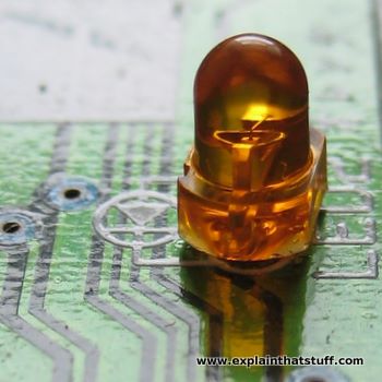
Photo: Unlike incandescent lamp bulbs (used in things like flashlights), which burn out relatively quickly, LEDs are extremely reliable—so much so, that they're typically soldered right onto electronic circuit boards. They virtually never wear out! This is the tiny LED indicator lamp from a computer printer's control panel.
If you know a bit about electricity,
you'll know that materials
fall broadly into two categories. There are some that let electricity
flow through them fairly well, known as conductors,
and others
that barely let electricity flow at all, known as insulators.
Metals
such as copper and gold are examples of good conductors, while
plastics and wood are typical insulators.
What's the difference between a conductor and an insulator?
Solids are joined together when their atoms
link up. In something like a plastic, the electrons in atoms are fully occupied binding
atoms into molecules and holding the molecules together. They're not
free to move about and conduct electricity. But in a conductor the
atoms are bound together in a different kind of structure. In metals,
for example, atoms form a crystalline structure (a bit like equal-sized marbles
packed inside a box) and some of their electrons remain free to
move throughout the whole material, carrying electricity as they go.
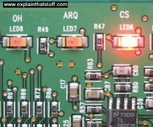
Photo: LEDs are much smaller than lamp bulbs and use a fraction as much energy. They are particularly suitable for use in instrument panels, which have to be lit up for hours at a time. Put many diodes together and you can make as much light as a conventional bulb and still save energy.
Sponsored links
How semiconductors work
Not everything falls so neatly into the two categories of
conductor or insulator. Put a big enough voltage across any material
and it will become a conductor, whether it's normally an insulator or
not. That's how lightning works. When a cloud moves through the air
picking up electric charge, it creates a massive voltage between
itself and the ground. Eventually, the voltage is so big that the
air between the cloud and the ground (which is normally an insulator)
suddenly "breaks down" and becomes a conductor—and you get a
massive zap of lightning as electricity flows through it.
Certain elements found in the middle of the periodic
table (the orderly grouping of chemical elements) are
normally insulators, but we can turn them into conductors with a
chemical process called doping.
We call these materials semiconductors and silicon and germanium are
two of the best known examples.
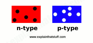
Silicon is normally an insulator, but if you add a
few atoms of the element antimony, you effectively sprinkle in some
extra electrons and give it the power to conduct electricity. Silicon
altered in this way is called n-type (negative-type) because
extra electrons (shown here as black blobs) can carry negative electric
charge through it.
In the same way, if you add
atoms of boron, you effectively take away electrons from the silicon
and leave behind "holes" where electrons
should be. This type of
silicon is called p-type (positive type) because the holes (shown here
as white blobs) can move
around and carry positive electric charge.
Artwork: N-type silicon has extra electrons (black blobs), while p-type silicon has a lack of electrons that we can think of as "extra holes" (white blobs).
How a junction diode works
Interesting things happen when you start putting p-type and n-type
silicon together. Suppose you join a piece of n-type silicon (with
slightly too many electrons) to a piece of p-type silicon (with
slightly too few). What will happen? Some of the extra electrons in
the n-type will nip across the join (which is called a junction) into the holes in the p-type
so, either side of the junction, we'll get normal silicon forming
again with neither too many nor too few electrons in it. Since
ordinary silicon doesn't conduct electricity, nor does this junction.
Effectively it becomes a barrier between the n-type and p-type
silicon and we call it a depletion zone
because it contains no free electrons or holes:
Suppose you connect a battery to this little p-type/n-type junction.
What
will happen? It depends which way the battery is connected. If you
put it so that the battery's negative terminal joins the n-type
silicon, and the battery's positive terminal joins the p-type
silicon, the depletion zone shrinks drastically.
Electrons and holes move across the junction in opposite
directions and a current flows. This is called forward-bias:
However, if you reverse the current, all that happens is that the
depletion zone gets wider. All the holes push up toward one end, all
the electrons push up to the other end, and no current flows at all.
This is called reverse-bias:
That's how an ordinary diode works and why it allows an electric
current will flow through it only one way. Think of a diode as an
electrical
one-way street. (Transistors,
incidentally, take the junction idea a step further by
putting three different pieces of semiconducting material side by side
instead of two.)
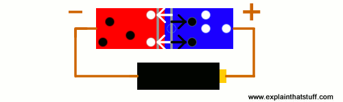
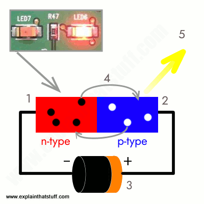
How LEDs work
LEDs are simply diodes that are designed to give off light. When a
diode is forward-biased so that electrons and holes are zipping back
and forth across the junction, they're constantly combining and
wiping one another out. Sooner or later, after an electron moves from
the n-type into the p-type silicon, it will combine with a hole and
disappear. That makes an atom complete and more stable and it gives
off a little burst of energy (a kind of "sigh of relief") in the
form of a tiny "packet" or photon of light.
This diagram summarizes what happens:
N-type silicon (red) has extra electrons (black).
P-type silicon (blue) has extra holes (white).
Battery connected across the p-n junction makes the diode forward biased, pushing electrons from
the n-type to the p-type and pushing holes in the opposite direction.
Electrons and holes cross the junction and combine.
Photons (particles of light) are given off as the electrons and holes recombine.
Types of LEDs
Photos (above and below): LEDs are transparent so light will pass
through them. You can see the two electrical contacts at one end
and the rounded lens at the other end. The lens helps the LED to produce a bright, focused beam of light—just like a miniature light bulb.
LEDs are specifically designed so they make light of a certain
wavelength and they're built into rounded plastic bulbs to make this
light brighter and more concentrated. Red LEDs produce light
with a wavelength of about 630–660 nanometers—which happens to look
red when we see it, while blue LEDs produce light with shorter
wavelengths of about 430–500 nanometers, which we see as blue.
You can also get LEDs that make invisible infrared light, which is
useful in things like "magic eye" beams that trigger
photoelectric cells
in things like optical smoke detectors and
intruder alarms. Semiconductor lasers work in a similar
way to LEDs but make purer and more precise beams of light.
Photo: Colored LEDs produce different wavelengths of light.
Red LEDs produce longer wavelengths of about 630–660 nanometers (nm), yellow come in at 555–600nm, and
green are shorter again at about 515–555nm. Outside the visible spectrum, infrared LEDs make
wavelengths greater than about 1000nm, while ultraviolet LEDs are often shorter than 400nm.
Who invented LEDs?
Whom should we thank for this fantastic little invention? Nick Holonyak: he came up with the idea of the light-emitting diode in 1962 while he was working for the General Electric Company. You might like to watch a short (4-minute) video about
Nick Holonyak's life and work and his thoughts about
the future of LEDs (courtesy of the Lemelson Foundation); if you're feeling more technically minded, you can read all about the solid-state physics behind LEDs in the patents listed in the references below.
What's so good about LEDs?
In a nutshell:
They're tiny and relatively inexpensive.
They're easy to control electronically.
They last virtually forever. That makes them brilliant for traffic signals.
They make light electronically without getting hot and that means they save lots of energy.
Photo: The red LEDs shining down from the top of this container are
being used to test a way of growing potatoes in space. LEDs are more suitable than ordinary light because
they don't produce heat (which would make the plants dry out).
The red light these LEDs produce makes the plants photosynthesize (produce growth from light and water) more efficiently.
Photo by courtesy of Marshall Space Flight Center (NASA-MSFC) and Internet Archive.
What next for LEDs?
It's the best part of five decades since Nick Holonyak invented the LED, but the technology is still developing.
In the 1970s, scientists discovered they could make LEDs from organic (carbon-based) materials, giving rise
to OLEDs (organic LEDs) that are now becoming popular in thin, flat, and sometimes even flexible displays. Two decades later, three Japanese-born scientists (Isamu Akasaki, Hiroshi Amano, and Shuji Nakamura)
invented blue-light-emitting diodes using the semiconductor gallium nitride,
earning them the Nobel Prize in Physics in 2014. Red and green LEDs had been around for
years—if you can remember early digital watches, you'll know their LED displays were always red—but blue light had always proved elusive. The conquest of the blue LED made it possible to produce perfect white light (either by
combining red, green, and blue LEDs or by shining blue light through a white phosphor), so enabling
energy-efficient LED lamps to compete effectively with older and less efficient technologies
like incandescent bulbs and
compact fluorescent lamps (CFLs). Gallium-nitride LEDs are also now finding their way into full-size color displays: they're very much brighter and considerably more efficient than rival
LCD displays and OLEDs, though not so good at large screen sizes.
Artwork: The structure of an early design for a blue-light LED built from multiple layers on a sapphire (Al2O3 substrate. The numbers in the figure indicate: 1 = the sapphire substrate; 2 = aluminum nitride buffer layer; 3 = n-type layer made from gallium nitride doped with silicon; 4 = semi-insulating, semi-p-type layer made from indium gallium nitride; 5 = p-type aluminum gallium nitride clad layer; 6 = p-type layer made of gallium nitride doped with magnesium ; 7 = aluminum positive electrode; 8 = aluminum negative electrode; 9 = insulating groove between electrodes. The LED emits light downward in this case, as shown by the yellow arrow. Artwork from US Patent 5,862,167: Light-emitting semiconductor device using gallium nitride compound by Michinari Sassa et al (co-authors include the Nobel-Prize winners Isamu Akasaki and Hiroshi Amano), courtesy of US Patent and Trademark Office.
Another new development in this area is the microLED display, made from very bright, very efficient LEDs with much higher pixel density than the screens currently used in things like laptops and smartphones. Although microLEDs are still a very new technology, they're expected to find applications in things like heads-up displays for
virtual reality and augmented reality
and smartphone screens that use much less battery power.
MAKE presents: The LED: A friendly 5-minute video introduction from MAKE's quirky Collin Cunningham. Collin explains how LEDs were discovered and shows how to make one of your own!
[PDF] Blue LEDs—Filling the world with new light: An easy-to-understand account of how three Japanese-born scientists scooped the 2014 Nobel Prize in Physics with the development of energy-efficient, blue gallium nitride LEDs.
Projects
Instructables: LED projects: Inexpensive, funky, and safe, LEDs are great for all kinds of electronic projects—and are particularly good for teaching kids about simple electronic circuits.
MAKE: Electronics by Charles Platt. O'Reilly, 2015. A clear and simple, hands-on introduction to electronics.
Technical books
Understanding Modern Transistors and Diodes by David L. Pulfrey. Cambridge University Press, 2010. Comprehensive textbook for undergraduates and graduate students. Explains the solid-state theory behind transistors and diodes, including applications such as solar cells, LEDs, memories, and power transistors.
Light-Emitting Diodes by E. Fred Schubert. Cambridge University Press/E. Fred Schubert, 2018. Opens with the history and theory of LEDs before covering their electrical and optical properties, packaging, and uses.
Nobel Shocker: RCA Had the First Blue LED in 1972 by Neel V. Patel. IEEE Spectrum, October 9, 2014. Although blue LEDs have only recently hit the headlines, they were first created almost half a century ago.
How Lasers Inspired the Inventor of the LED by Nathan Hurst. Wired, October 9, 2012. A brief interview with Nick Holonyak about the invention and future development of LEDs.
50 Years of LED Technology by Roberto Baldwin. Wired, October 8, 2012. A fascinating photo gallery of the benefits LEDs have brought to many areas of modern life.
The Lightbulb That Really Is a Better Idea by Paul Wallich. IEEE Spectrum, December 30, 2010. What are the prons and cons (and the technical challenges) of building LEDs into a conventional, energy-saving lamp?
US Patent 3,936,855: Light-emitting diode fabrication process by James Emanuel Goell et al, International Telephone and Telegraph Corporation. Issued Feb 3, 1976. How are LEDs made? This patent outlines one method of making them developed in the early 1970s.
Please do NOT copy our articles onto blogs and other websites
Articles from this website are registered at the US Copyright Office. Copying or otherwise using registered works without permission, removing this or other copyright notices, and/or infringing related rights could make you liable to severe civil or criminal penalties.