Molecular beam epitaxy
by Chris Woodford. Last updated: October 25, 2022.
Growing crystals is easy. Fill a plastic bottle almost to the top with cold water and place it in a freezer for a couple of hours. Take it out again at just the right time and the water will still be a liquid but, if you tilt the bottle very gently, it will snap into an amazing snow forest of ice crystals right before your eyes! Growing single crystals for scientific or industrial use in such things as integrated circuits is somewhat harder because you need to combine atoms of different chemical elements much more precisely. At the opposite end of the spectrum from growing random ice crystals in your freezer, one of the most exacting methods of making a crystal is a technique called molecular beam epitaxy (MBE). It sounds horribly complex, but it's fairly easy to understand. Let's take a closer look!
Photo: Molecular beam epitaxy (MBE) being used to make photovoltaic solar cells: You can see the beams around the edge that fire molecules onto the substrate in the center. Photo by Jim Yost courtesy of US DOE/NREL (U.S. Department of Energy/National Renewable Energy Laboratory).
Sponsored links

Contents
What is molecular beam epitaxy?
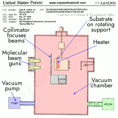
To make an interesting new crystal using MBE, you start off with a base material called a substrate, which could be a familiar semiconductor material such as silicon, germanium, or gallium arsenide. First, you heat the substrate, typically to some hundreds of degrees (for example, 500–850°C or about 930–1560°F in the case of gallium arsenide). [1]
Then you fire relatively precise beams of atoms or molecules (heated up so they're in gas form) at the substrate from "guns" called effusion cells. Each effusion cell is open at one end and consists of a tapering crucible (a kind of heat-resistant cup) filled with the material it's going to "fire," an electrically controlled heater, and a thermocouple for measuring and regulating its temperature. [2] The number of cells depends on the complexity of the crystal being produced; there can be as many as 8–14 of them. [3] Like the substrate, the cells are heated to high temperatures—a maximum of about 1500–1600°C or so (2700–2900°F). [4]
Artwork: A typical effusion cell is a cone-shaped, electrically heated crucible, usually made from pyrolitic boron nitride (PBN), which can withstand high temperatures and low pressures. Its temperature is measured and controlled using a thermocouple, mounted at its base. The evaporant (the substance being fired out as a molecular beam) sits at the bottom of the crucible. A heat sink (blue) and radiative insulation (yellow) help to stop nearby effusion cells from affecting one another.
You need one cell for each different beam, shooting a different kind of molecule at the substrate, depending on the nature of the crystal you're trying to create. The molecules land on the surface of the substrate, condense, and build up very slowly and systematically in ultra-thin layers, so the complex, single crystal you're after grows one atomic layer at a time. (Very slowly means very slowly, typically at a rate of a few microns, or fractions of microns, per hour.) [5] That's why MBE is an example of what's called thin-film deposition. Since it involves building up materials by manipulating atoms and molecules, it's also a perfect example of what we mean by nanotechnology.
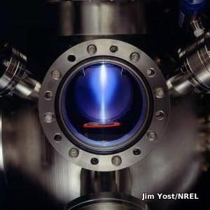
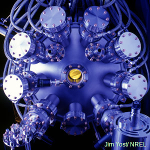
Photo: Molecular beam epitaxy (MBE) in action. MBE takes place in ultra-high vacuum (UHV) chambers like this, at temperatures of around 500°C (932°F), to ensure a totally clean, dust-free environment; the slightest contamination could ruin the crystal. Photo by Jim Yost courtesy of US DOE/NREL (U.S. Department of Energy/National Renewable Energy Laboratory).
One reason that MBE is such a precise way of making a crystal is that it happens in highly controlled conditions: extreme cleanliness and what's called an ultra-high vacuum (UHV), so no dirt particles or unwanted gas molecules can interfere with or contaminate the crystal growth. "Extreme cleanliness" means even cleaner than the conditions used in normal semiconductor manufacture; an "ultra-high vacuum" means the pressure is so low that it's at the limit of what's easily measurable—as little as one hundred trillionth of atmospheric pressure! [6]
That's pretty much MBE in a nutshell. If you want a really simply analogy, it's a little bit like the way an inkjet printer makes layers of colored print on a page by firing jets of ink from hot guns. In an inkjet printer, you have four separate guns firing different colored inks (one for cyan ink, one for magenta, one for yellow, and one for black), which slowly build up a complex colored image on the paper. In MBE, separate beams fire different molecules and they build up on the surface of the substrate, albeit more slowly than in inkjet printing—MBE can take hours! Epitaxially simply means "arranged on top of," so all molecular beam epitaxy really means is using beams of molecules to build up layers on top of a substrate.
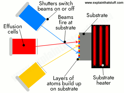
Photo: Molecular beam epitaxy (MBE) means creating a single crystal by building up orderly layers of molecules on top of a substrate (base layer). This bit of apparatus is called a growth chamber. It's only one part of an MBE machine, which typically includes multi chambers (introduction and extraction chambers, two or more growth chambers, an analysis chamber, and a preparation chamber), all kept at ultra-high vacuum (UHV).