What's the smallest thing you've ever
seen? Maybe a hair, a pinhead, or a spec of dust? If you swapped your eyes for a
couple of the world's most powerful microscopes, you'd be able to see
things 100 million times smaller: bacteria, viruses, molecules—even
the atoms in crystals would be clearly visible to you!
Ordinary optical microscopes (light-based microscopes), like the ones you find in a school
lab, are nowhere near good enough to see things in such detail. It
takes a much more powerful electron microscope—using beams of
electrons instead of rays of light—to take us down to
nano-dimensions. Let's take a
closer look at electron microscopes and how they work!
Photo: This Hitachi S-4700 field-emission, scanning electron microscope
can magnify over half a million times and resolve features just 2 nanometers across!
By courtesy of NASA Glenn Research Center and
Internet Archive.
We can see objects in the world around us because
light rays (either from the Sun or from another light source, like a
desktop lamp) reflect off them and into our eyes. No-one really knows
what light is like, but scientists have settled on the idea that it
has a sort of split personality. They like to call this
wave-particle duality, but the basic idea is much
simpler than it sounds. Sometimes light behaves like a train
of waves—much like waves traveling over the sea. Other times, it's
more like a
steady stream of particles—a bombardment of microscopic cannonballs, if
you like. You can read these words on your computer screen because
light particles are streaming out of the display
into your eyes in a
kind of mass, horizontal hailstorm! We call these individual
particles of light photons: each one is a
tiny packet of electromagnetic energy.
Seeing with photons is fine if you want to look at
things that are much bigger than atoms. But if you want to see things
that are smaller, photons turn out to be pretty clumsy and useless.
Just imagine if you were a master wood carver, renowned the world over for
the finely carved furniture you made. To carve such fine details,
you'd need small, sharp, precise tools smaller
than the patterns you wanted to make. If all you had were a sledgehammer and a
spade, carving intricate furniture would be impossible. The basic rule
is that the tools you use have to be smaller than the things you're
using them on.
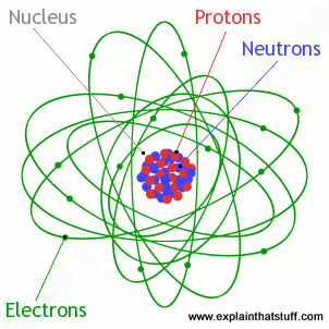
Photo: Inside an atom: electrons are the particles
in shells (orbitals) around the nucleus (center).
And the same goes for science. The smallest thing you can see with a microscope
is determined (partly) by the light that shines through it. An ordinary light microscope
uses photons of light, which are equivalent to waves with a wavelength
of roughly 400–700 nanometers.
That's fine for studying something like a human hair, which is about
100 times bigger (50,000–100,000 nanometers in diameter).
But what about a bacteria that's 200 nanometers across
or a protein just 10 nanometers long?
If you want to see finely detailed things that are "smaller than light"
(smaller than the wavelength of photons), you need to use particles
that have an even shorter wavelength than photons: in other
words, you need to use electrons.
As you probably know, electrons are the minute charged particles that
occupy the outer regions of atoms. (They're also the particles that
carry electricity around circuits.) In
an electron microscope, a stream of electrons takes the place of a beam of light.
An electron has an equivalent wavelength of just over 1 nanometer, which
allows us to see things smaller even than light itself
(smaller than the wavelength of light's photons).
Sponsored links
How electron microscopes work
If you've ever used an ordinary microscope, you'll
know the basic idea is simple. There's a light at the bottom that
shines upward through a thin slice of the specimen. You look through
an eyepiece and a powerful lens to see a considerably magnified
image of the specimen (typically 10–200 times bigger). So there
are essentially four important parts to an ordinary microscope:
The source of light.
The specimen.
The lenses that makes the specimen seem bigger.
The magnified image of the specimen that you see.
In an electron microscope, these four things are
slightly different.
The light source is replaced by a beam of
very fast moving electrons.
The specimen usually has to be specially
prepared and held inside a vacuum chamber from which the air has
been pumped out (because electrons do not travel very far in air).
The lenses are replaced by a series of
coil-shaped electromagnets through which the electron beam travels.
In an ordinary microscope, the glass lenses bend (or refract) the
light beams passing through them to produce magnification. In an
electron microscope, the coils bend the electron beams the same way.
The image is formed as a photograph (called an electron
micrograph) or as an image on a TV
screen.
That's the basic, general idea of an electron microscope. But there
are actually quite a few different types of electron
microscopes and they all work in different ways. The three most
familiar types are called transmission electron microscopes (TEMs), scanning
electron microscopes (SEMs), and scanning tunneling microscopes
(STMs).
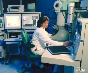
Photo: 1) Studying a specimen with a transmission electron microscope.
The electron gun is in the tall gray tube at the top.
By courtesy of NASA
Glenn Research Center and
Internet Archive.
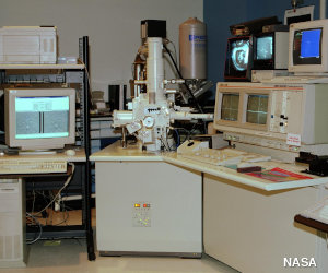
2) A typical scanning electron microscope.
The main microscope equipment is in the center.
You can see the image it produces on the screen on the left.
By courtesy of NASA Langley Research Center
and Internet Archive.
Transmission electron microscopes (TEMs)
A TEM has a lot in common with an ordinary optical
microscope. You have to prepare a thin slice of the specimen quite
carefully (it's a fairly laborious process) and sit it in a vacuum
chamber in the middle of the machine. When you've done that, you fire
an electron beam down through the specimen from a giant electron gun
at the top. The gun uses electromagnetic coils and high voltages
(typically from 50,000 to several million volts) to accelerate the
electrons to very high speeds. Thanks to our old friend wave-particle
duality, electrons (which we normally
think of as particles) can behave like waves (just as waves of light
can behave like particles). The faster they travel, the smaller the
waves they form and the more detailed the images they show up. Having
reached top speed, the electrons zoom through the specimen and out
the other side, where more coils focus them to form an image on
screen (for immediate viewing) or on a photographic plate (for making
a permanent record of the image). TEMs are the most powerful electron
microscopes: we can use them to see things just 1 nanometer in
size, so they effectively magnify by a million times or more.
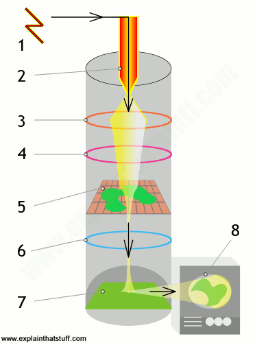
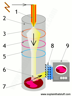
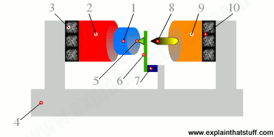
How a transmission electron microscope (TEM) works
A transmission electron microscope fires a beam of electrons through a specimen to produce a magnified
image of an object.
A high-voltage electricity supply powers the cathode.
The cathode is a heated filament, a bit like the electron gun in an old-fashioned cathode-ray tube (CRT) TV. It generates a beam
of electrons that works in an analogous way to the beam of light in an optical microscope.
An electromagnetic coil (the first lens) concentrates the electrons into a more powerful beam.
Another electromagnetic coil (the second lens) focuses the beam onto a certain part of the specimen.
The specimen sits on a copper grid in the middle of the main microscope tube. The beam passes through the specimen and "picks up"
an image of it.
The projector lens (the third lens) magnifies the image.
The image becomes visible when the electron beam hits a fluorescent screen at the base of the machine. This is analogous to
the phosphor screen at the front of an old-fashioned TV .
The image can be viewed directly (through a viewing portal), through binoculars at the side, or on a TV monitor
attached to an image intensifier (which makes weak images easier to see).
Scanning electron microscopes (SEMs)
Most of the funky electron microscope images you
see in books—things like wasps holding microchips in their
mouths—are not made by TEMs but by scanning electron microscopes
(SEMs), which are designed to make images of the surfaces
of
tiny objects. Just as in a TEM, the top of a SEM is a powerful
electron gun that shoots an electron beam down at the specimen. A
series of electromagnetic coils pull the beam back and forth,
scanning it slowly and systematically across the specimen's surface.
Instead of traveling through the specimen, the electron beam
effectively bounces straight off it. The electrons that are reflected
off the specimen (known as secondary electrons) are directed at a
screen, similar to a cathode-ray TV screen,
where they create a TV-like picture. SEMs are generally about 10
times less powerful than TEMs (so we can use them to see things about
10 nanometers in size). On the plus side, they produce very sharp, 3D
images (compared to the flat images produced by TEMs) and their
specimens need less preparation.
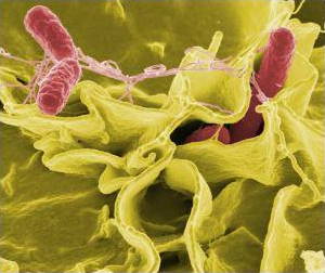
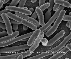
Photo: Typical images produced by a SEM.
1) An artificially colored, scanning electron micrograph showing Salmonella
typhimurium (red) invading cultured human cells.
2) A scanning electron micrograph of the bacteria Escherichia coli
(E.coli). Photos by courtesy of Rocky Mountain Laboratories,
US National Institute of Allergy and Infectious Diseases (NIAID),
and US National Institute of Health.
Sponsored links
How a scanning electron microscope (SEM) works
A scanning electron microscope scans a beam of electrons over a specimen to produce a magnified
image of an object. That's completely different from a TEM, where the beam of electrons goes right through the specimen.
Electrons are fired into the machine.
The main part of the machine (where the object is scanned) is contained within a sealed vacuum chamber because precise electron beams can't travel effectively through air.
A positively charged electrode (anode) attracts the electrons and accelerates them into an energetic beam.
An electromagnetic coil brings the electron beam to a very precise focus, much like a lens.
Another coil, lower down, steers the electron beam from side to side.
The beam systematically scans across the object being viewed.
Electrons from the beam hit the surface of the object and bounce off it.
A detector registers these scattered electrons and turns them into a picture.
A hugely magnified image of the object is displayed on a TV screen.
Photo: A scanning transmission electron microscope (STEM) has things in
common with both TEMs and SEMs. Like a TEM, the electron beam passes through the sample.
Like a SEM, the beam is narrowly focused and can be scanned across the sample to make a TV-screen image.
Photo by Jim Yost courtesy of US
Department of Energy/National Renewable Energy Laboratory (NREL).
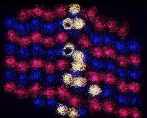
Among the newest electron microscopes, STMs were
invented by Gerd Binnig and
Heinrich Rohrer in 1981. Unlike TEMs, which produce images of the
insides of materials, and SEMs, which show up 3D surfaces, STMs are
designed to make detailed images of the atoms or molecules on the
surface of something like a crystal. They work differently to TEMs
and SEMs too: they have an extremely sharp metallic probe that scans
back and forth across the surface of the specimen. As it does so,
electrons try to wriggle out of the specimen and jump across the gap,
into the probe, by an unusual quantum phenomenon called "tunneling." The closer the probe is to
the surface, the easier it is for electrons to tunnel into it, the
more electrons escape, and the greater the tunneling current. The
microscope constantly moves the probe up or down by tiny
amounts to keep the tunneling current constant. By recording how
much the probe has to move, it effectively measures the peaks and
troughs of the specimen's surface. A computer turns this information
into a map of the specimen that shows up its detailed
atomic structure. One big drawback of ordinary electron microscopes
is that they produce amazing detail using high-energy beams of electrons,
which tend to damage the objects they're imaging. STMs avoid this
problem by using much lower energies.
How a scanning tunneling microscope (STM) works
A scanning tunnelling microscope makes images using electrons that "tunnel" between the probe
and the specimen. Here's how it works:
The sample (blue) is sealed inside a vacuum chamber.
The chamber is cooled
down to almost absolute zero by a cryogenic source, such as a liquid helium refrigerator.
A pump creates a very high vacuum in the chamber.
The sample being scanned serves as one electrode.
The probe tip, an incredibly small distance above, serves as the other electrode. The two electrodes
can be scanned past one another by a drive that moves in three dimensions.
The tunneling current output from the probe is analyzed by a measuring device.
Results can be displayed on a screen or plotter,
showing up (in this case) the pattern of atoms on the surface of the sample.
If you think STMs are amazing, AFMs (atomic force microscopes), also invented by Gerd Binnig, are even better!
One of the big drawbacks of STMs is that they rely on electrical currents
(flows of electrons) passing through materials, so they can only make images of conductors.
AFMs don't suffer from this problem because, although they use still tuneling, they don't
rely on a current flowing between the specimen and a probe, so we can use them to make atomic-scale images of materials such as plastics, which don't conduct electricity.
Photo: A typical atomic force microscope (AFM)—the Dimension Icon® made by Bruker. Photo by Donna M Lindner courtesy of Air Force Research Laboratory
and DVIDS.
An AFM is a microscope with a little arm called a cantilever with a tip on the end
that scans across the surface of a specimen. As the tip sweeps across the surface, the force between the atoms from which it's made
and the atoms on the surface constantly changes, causing the cantilever to bend by minute amounts.
The amount by which the cantilever bends is detected by bouncing a laser beam off its surface.
By measuring how far the laser beam travels, we can measure how much the cantilever bends and the forces
acting on it from moment to moment, and that information can be used to figure out and plot
the contours of the surface. Other versions of AFMs (like the one illustrated here) make an image by measuring a current that "tunnels" between the scanning tip and a tunneling probe mounted just behind it.
AFMs can make images of things at the atomic level and they can also be used to manipulate individual atoms and
molecules—one of the key ideas in nanotechnology.
How an atomic force microscope (AFM) works
An atomic force microscope is similar to a scanning tunnelling microscope, but makes images using a tiny cantilever probe that's wiggled about by the force between itself and the specimen.
Here's how one version works:
The specimen to be scanned (1) is mounted on a drive mechanism (2) that can move it in three dimensions.
To prevent unwanted vibrations, that mechanism is fixed to a rubber cushion (3) mounted on a firm aluminum base (4), which is further cushioned by multiple layers of aluminum plates and rubber pads (not shown).
To create an image, the specimen is slowly moved around the sharp, fixed imaging point (5), which is mounted on a spring cantilever made of thin gold foil (6), attached to a
piezoelectric crystal (7), and fixed to the same aluminum base.
At the other end of the apparatus, a tunneling probe (8) is moved very close (to within about 0.3nm) of the spring cantilever by a second drive mechanism (9), isolated by another rubber cushion (10).
As the sample (1) moves around the imaging point (5), the current that tunnels between the spring cantilever (6) and the tunneling tip (8) is constantly measured. These measurements are converted into data that can be used to draw a detailed surface map of the specimen.
Here's a brief history of the key moments in electron microscopy—so far!
1924: French physicist Louis de Broglie
(1892–1987) realizes that electron beams have a wavelike nature similar
to light. Five years later, he wins the Nobel Prize in Physics for this work.
1931: German scientists Max Knoll
(1897–1969) and his pupil Ernst Ruska (1906–1988) build the first
experimental TEM in Berlin.
1933: Ernst Ruska builds the first electron microscope that is
more powerful than an optical microscope.
1935: Max Knoll builds the first crude SEM.
1935: Working at the University of Toronto, James Hillier and Albert Prebus build on Ruska's work to produce the first commercially successful TEM for RCA in North America.
1941: German electrical engineers Manfred Von Ardenne and Bodo von Borries patent an "electron scanning microscope" (SEM).
1965: Cambridge Instrument Company
produces the first commercial SEM in England.
1981: Gerd Binnig (1947–) and Heinrich Rohrer (1933–) of IBM's Zurich Research Laboratory invent the
STM and produce detailed images of atoms on the surface of a crystal of gold.
1985: Binnig and his colleague Christoph Gerber produce the first atomic force microscope (AFM)
by attaching a diamond to a piece of gold foil.
1986: Binnig and Rohrer share the Nobel Prize in Physics with the original pioneer of
electron microscopes, Ernst Ruska.
1989: The first commercial AFM is produced by Sang-il Park (founder of Park Systems of Palo Alto, California).
Flickr: Scanning electron microscopy: A Flickr group pool of several hundred SEM images. Some of these are copyright, others are published under various Creative Commons licences permitting you to reuse them under certain conditions.
Videos
Atomic force microscope (AFM) at work!: A great little video showing the cantilever and tip of an atomic force microscope (AFM) in action. Note the green ruler scale on the left, which shows you
the scale at which we're working as we zoom in and out.
Books
Easy reading
Heaven and Earth: Unseen by the Naked Eye:
By David Malin, Katherine Roucoux. Phaidon Press, 2007. Lots of stunning photos of the very big and very small in
this excellent coffee table book.
Cool Stuff and How it Works:
By Chris Woodford et al. Dorling Kindersley, 2005. One of my own books, this one explains all sorts of everyday objects with stunning photography (and quite a few electron micrographs).
Cool Stuff 2.0 (The Gadget Book):
By Chris Woodford and Jon Woodcock. Dorling Kindersley, 2007. A follow-up to Cool Stuff, with more stunning photos (and a few more electron micrographs).
The Evolution of the Microscope by S. Bradbury.
Elsevier, 2014. A reprint of a 1967 book. The early history is obviously still applicable, but the final chapter about electron microscopes is now a little dated.
Power Tool for Making Nanoscale Objects by Saswato Das. IEEE Spectrum, July 1, 2007. Introducing a micro-manufacturing technique called transmission electron beam ablation lithography (TEBAL).
Patents
A patent search is a good way of finding deeper technical details and drawings. Here are a few key patents for starters:
US Patent 3,191,028: Electron scanning microscope
by Manfred Von Ardenne and Bodo von Borries, patented May 13, 1941. I think this is the original SEM patent, building on earlier work by Ruska and Knoll.
US Patent 3,191,028: Scanning electron microscope
by Albert V. Crewe, US Atomic Energy Commission, patented June 22, 1965. A higher magnification and resolution SEM design from the mid-1960s. This is a much more detailed description than the Ardenne patent with some great technical drawings.
Please do NOT copy our articles onto blogs and other websites
Articles from this website are registered at the US Copyright Office. Copying or otherwise using registered works without permission, removing this or other copyright notices, and/or infringing related rights could make you liable to severe civil or criminal penalties.
Woodford, Chris. (2007/2024) Electron microscopes. Retrieved from https://www.explainthatstuff.com/electronmicroscopes.html. [Accessed (Insert date here)]
Bibtex
@misc{woodford_electron-microscopes,
author = "Woodford, Chris",
title = "Electron microscopes",
publisher = "Explain that Stuff",
year = "2007",
url = "https://www.explainthatstuff.com/electronmicroscopes.html",
urldate = "2024-04-03"
}